Photo-induced intramolecular charge transfer in an ambipolar field-effect transistor based on a π-conjugated donor–acceptor dyad

Schematic view of intramolecular charge transfer by photoabsorption in ambipolar organic semiconductor

Our research team collaborated in a photoconductivity characterization of an interesting dyad molecule. A π-conjugated tetrathiafulvalene-fused perylenediimide (TTF-PDI) molecular dyad is successfully used as a solution-processed active material for light sensitive ambipolar field-effect transistors with balanced hole and electron mobilities. The photo-response of the TTF-PDI dyad resembles its absorption profile. Wavelength-dependent photoconductivity measurements reveal an important photo-response at an energy corresponding to a PDI-localized electronic π–π* transition and also a more moderate effect due to an intramolecular charge transfer from the HOMO localized on the TTF unit to the LUMO localized on the PDI moiety. This work clearly elucidates the interplay between intra- and intermolecular electronic processes in organic devices. More details can be found in original paper.

Posted in Research | Leave a comment

Extreme sensitivity to adsorbates of Time-of-Flight photoconductivity in graphene

We have examined the effect of submonolayer coverage of 1-pyrene butyric acid on charge carrier transport in reduced graphene oxide. We have modeled the interaction of 1-pyrene butyric acid molecules with graphene and determined the amount of charge transfer at the interface between the two materials. The effect of 1-pyrene butyric acid as electron acceptor was determined by transfer characteristics measurements on thin film transistors for thick layers. By using time-resolved photocurrent measurements we were able to detect a reduction of electron mobility in reduced graphene oxide for coverage as low as 0.08%. These results were published in Organic Electronics.

Posted in Uncategorized | Leave a comment

Graphene Workshop

We are proud to announce Graphene Workshop 2013 – from fundamental properties to application, which will be hosted in our Laboratory from 8th to 11th April 2013.

Posted in Media | Leave a comment

Grafold-driven nucleation of pentacene on graphene

Pentacene on Graphene

Elongated islands of pentacene on graphene surface. The nucleation of pentacene is initialized and driven by grafolds.

Folds in graphene – grafolds are frequently present even after transferring graphene layers, which were fabricated by chemical vapor deposition (CVD), onto SiO2 substrates. As we are showing in the present Letter, grafolds have a crucial role in determining the morphology of pentacene layers on graphene, and should be as such considered in designing fabrication protocols of pentacene-graphene devices. Our atomic force microscopy investigation of the initial stages of growth of vacuum-evaporated pentacene on CVD graphene shows three-dimensional growth at submonolayer coverages of pentacene. Moreover, islands were found to preferentially nucleate at the location of the grafolds. We interpret this behavior in terms of increased chemical reactivity of grafolds that was predicted in previous theoretical works. These results were published here.

Posted in Uncategorized | Leave a comment

Time-of-flight mobility of charge carriers in position-dependent electric field

Comparison between time-of-flight photocurrent in an infinite parallel electrodes setup and coplanar electrodes setup.

We explained the difference between charge mobility of time-of-flight measurement and field-effect measurement in a recent paper. Time-of-flight measurements of the photocurrent in thin organic semiconductor layers represent an effective way to extract charge carrier mobility. A common method to interpret the time-dependence of the photocurrent in these material systems assumes a position-independent electric field between two coplanar electrodes. In this letter, we compare time-dependence of the photocurrent, measured in the samples comprising thin layers of poly-3-hexylthiophene, with the Monte Carlo simulations. In the simulations, we have used both, a position-independent and a position-dependent electric field. We obtained a favorable agreement between the simulations and the measurements only in the case of position-dependent electric field. We demonstrate that the charge carrier mobility may be underestimated by more than one order of magnitude, if a position-independent electric field is used in the calculations of the mobility.

Posted in Research | Leave a comment

Scientific publication in the journal Nature reinforces the important role of Nova Gorica University in the field of organic electronics.

Optical image of thin-film transistor during photocurrent time response measurements.

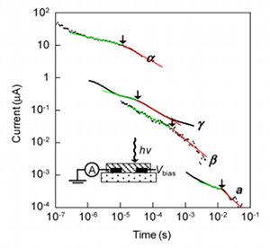
The researchers of Laboratory for Organic Matter Physics, University of Nova Gorica dr. Egon Pavlica and prof. dr. Gvido Bratina, together with colleagues from the University of Strasbourg, France, Humboldt University in Berlin, Germany and Stanford University, USA, have published an article in a prominent scientific journal Nature Chemistry on the June 24th. In the published work, they have presented the principle of operation and fabrication of a bi-stable photo-activated switch, which is based on a blend of two different organic semiconductor materials (Nature Chemistry, doi: 10.1038/nchem.1384). The discovery joins together the functionality of electric charge transport and the sensitivity to light into a single active layer, reducing the size and the complexity of a photo-modulated switch. The researches in the published work have prepared the blend of two different organic semiconductors: a derivative of the diarylethene molecule and a polyhexylthiophene polymer. Such blends exhibit bi-stable nature of electrical conductivity, which can be modulated with the light illumination. The conductivity can be switched from non-conducting to conducting state, when the blend layer is illuminated with the light of specific wavelength. When the blend is illuminated with the light of different wavelength, the conductivity switches from conductive to non-conductive state. In order to prove the principle of operation, a photo-switchable organic thin-film transistor was fabricated. The device photoresponse was found to be in the microsecond range, and thus on a technologically relevant timescale. This modular blending approach allows for the convenient incorporation of various molecular components, which opens up perspectives on multifunctional devices and logic circuits.

Posted in Research | Leave a comment

Single-step processing of TES-ADT based transistors

Optical microscopy of a thin TES-ADT layer presenting fantasy shapes.


Our lab was involved in a discovery of a simple, alternative route towards high-mobility structures of the small-molecular semiconductor 5,11-bis(triethyl silylethynyl) anthradithiophene – TES-ADT that requires one single processing step without the need for any post-deposition processing. The method relies on careful control of the casting temperature of the semiconductor and allows rapid production of transistors with uniform and reproducible device performance over large areas. More information can be found in the published paper.

Posted in Research | Leave a comment