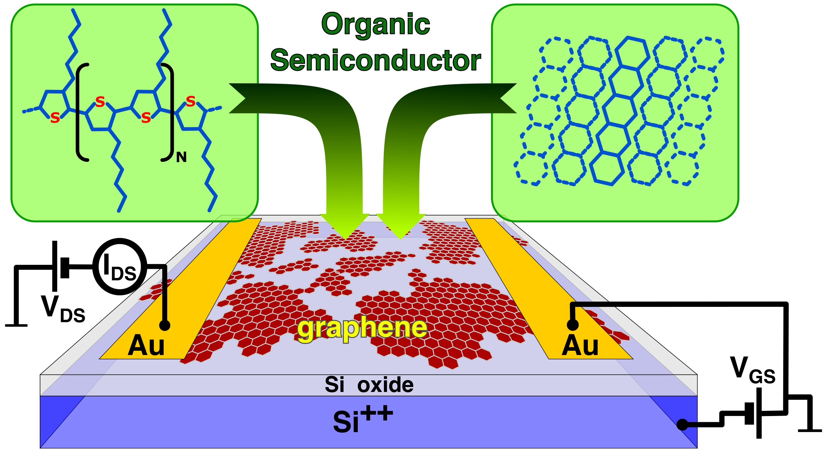

PDIF-CN2 on graphene
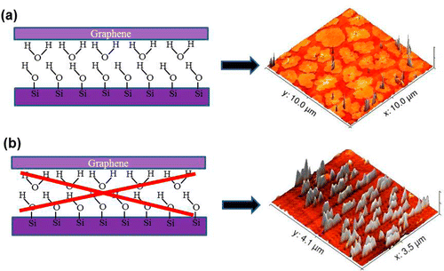
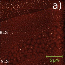
We have studied submonolayer coverages of N,N-1H,1H-perfluorobutyl dicyanoperylenecarboxydiimide (PDIF-CN2) on mechanically exfoliated graphene transferred onto SiO2 substrates. Our atomic force microscopy (AFM) data show that PDIF-CN2 forms irregularly-shaped 1.4 nm-high islands. From the selected area diffraction performed with transmission electron microscope (TEM) we conclude that this height corresponds to stacks of molecules, which are inclined for 43° relative to the graphene surface. AFM also showed complete absence of PDIF-CN2 on single-layer graphene (SLG). Electric force microscopy revealed a marked difference in surface charge density between a single-layer graphene and bilayer graphene, with a higher surface charge on SLG than on the bilayer graphene. We associate this behavior with type doping of graphene due to the electrostatic dipole induced by the molecular water layer present at the graphene/SiO2 interface. The crucial role of the graphene/SiO2 interface in determining growth of PDIF-CN2 was further confirmed by TEM examination of PDIF-CN2 deposited onto unsupported SLG. The results are published in Surface Science.