Self-suspended nanomesh scaffold for ultrafast flexible photodetectors based on organic semiconducting crystals

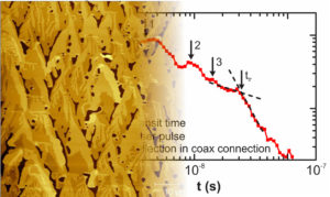
Our group was involved in a study of transient photocurrent responses of self‐standing nanostructures. These devices are of fundamental interest in materials science and nanoscience and are widely used in (opto‐)electronic and photonic devices as well as in micro‐electromechanical systems. To date, large‐area and self‐standing nanoelectrode arrays assembled on flexible substrates have not been reported. Here the fabrication of a hollow nanomesh scaffold on glass and plastic substrates with a large surface area over 1 mm2 and ultralow leakage current density (≈1–10 pA mm−2 @ 2 V) across the empty scaffold is demonstrated. Thanks to the continuous sub‐micrometer space formed in between the nanomesh and the bottom electrode, highly crystalline and dendritic domains of 6,13‐bis(triisopropylsilylethinyl)pentacene growing within the hollow cavity can be observed. The high degree of order at the supramolecular level leads to efficient charge and exciton transport; the photovoltaic detector supported on flexible polyethylene terephthalate substrates exhibits an ultrafast photoresponse time as short as 8 ns and a signal‐to‐noise ratio approaching 105. Such a hollow scaffold holds great potential as a novel device architecture toward flexible (opto‐)electronic applications based on self‐assembled micro/nanocrystals. Published in Advanced Materials.

Posted in Uncategorized | Leave a comment

Negative field-dependent charge mobility in crystalline organic semiconductors with delocalized transport

Charge-carrier mobility has been investigated by time-of-flight (TOF) transient photocurrent in a lateral transport configuration in highly crystalline thin films of 2,7-dioctyl[1]benzothieno [3,2-b][1] benzothiophene (C8-BTBT) grown by a zone-casting alignment technique. High TOF mobility has been revealed that it is consistent with the delocalized nature of the charge transport in this material, yet it featured a positive temperature dependence at ?≥295K. Moreover, the mobility was surprisingly found to decrease with electric field in the high-temperature region. These observations are not compatible with the conventional band-transport mechanism. We have elaborated an analytic model based on effective-medium approximation to rationalize the puzzling findings. The model considers the delocalized charge transport within the energy landscape formed by long-range transport band-edge variations in imperfect organic crystalline materials and accounts for the field-dependent effective dimensionality of charge transport percolative paths. The results of the model calculations are found to be in good agreement with experimental data. The work was published in Chemical Papers.

Posted in Uncategorized | Leave a comment

The effect of polymer molecular weight on the performance of PTB7-Th:O-IDTBR non-fullerene organic solar cells

Our group has been involved in a collaborative approach to study non-fullerene organic solar cells. Recent advances in the development of non-fullerene acceptors have increased the power conversion efficiency of organic solar cells to approximately 13%. Fullerene-derivatives and non-fullerene acceptors possess distinctively different structural, optical and electronic properties, which also change the requirements on the polymer donor in non-fullerene organic solar cells. Therefore, in this study, the effect of the molecular weight of the conjugated polymer on the photovoltaic performance, charge carrier mobility, crystallization properties, film morphology, and non-geminate recombination dynamics is systematically investigated in polymer:small molecule organic solar cells using the low bandgap polymer PTB7-Th as the donor and the non-fullerene indacenodithiophene-based small molecule O-IDTBR as the acceptor. Among the examined polymer samples (50–300 kDa), high molecular weights of PTB7-Th (with an optimum molecular weight of 200 kDa) are advantageous to achieve high efficiencies up to 10%, which can be correlated with an increased crystallinity, an improved field-effect hole mobility (1.05 × 10⁻² cm2 V−1 s−1), lower charge carrier trapping and a reduced activation energy of charge transport (98 meV). Bias-assisted charge extraction and transient photovoltage measurements reveal higher carrier concentrations (1016 cm−3) and long lifetimes (4.5 μs) as well as lower non-geminate recombination rate constants in the corresponding devices, supporting the high photocurrents (ca. 15.2 mA cm−2) and fill factors (>60%). Work was published in Journal of Materials Chemistry A.

Posted in Uncategorized | Leave a comment

Charge carrier transport in polycrystalline CH3NH3PbI3 perovskite thin films in a lateral direction characterized by time-of-flight photoconductivity.

We used time-of-flight photocurrent measurements to determine the role of grain boundaries in charge carrier transport in thin layers of methyl ammonium lead iodide (CH3NH3PbI3). The measurement results were compared to Kinetic Monte Carlo simulations, based on a transport model, which disentangles the transport within crystallites and hopping across grain boundaries. The observed mobilities of electrons are in the order ∼2.5 × 10−1 cm2V−1s−1. The hopping across grains is modeled with an Arrhenius-type probability rate, characterized by activation energy (Ea). It was found that the Ea estimated from the slope of a mobility-temperature dependence is in the range of ∼56–70 meV. The factors contributing to Ea are shunting pathways and the grain-size variations including energy level misalignments at the grain boundaries. These results represent a step toward a design of novel windowless organic-inorganic perovskite solar cells. More is published in Materials Chemistry and Physics.

Posted in Uncategorized | Leave a comment

Fast-response photonic device based on organic-crystal heterojunctions assembled into a vertical-yet-open asymmetric architecture.

Our group was involved in collaboration to investigate fast photocurrent transients of crystalline dioctyl‐3,4,9,10‐perylenedicarboximide nanowires and 6,13‐bis(triisopropylsilylethynyl) pentacene microplates , which were integrated into a vertical‐yet‐open asymmetrical heterojunction for the realization of a high‐performance organic photovoltaic detector, which shows fast photoresponse, ultrahigh signal‐to‐noise ratio, and high sensitivity to weak light. More of this interesting research can be found in Advanced Materials.

Posted in Uncategorized | Leave a comment

The role of local potential minima on charge transport in thin organic semiconductor layers

We have performed a systematic study of dependence of time-resolved photocurrent on the point of charge excitation within the organic semiconductor channel formed by two coplanar metal electrodes. The results confirm that spatial variation of electric field between the electrodes crucially determines transport of photogenerated charge carriers through the organic layer. Time-of-flight measurements of photocurrent demonstrate that the transit time of photogenerated charge carrier packets drifting between the two electrodes decreases with increasing travelling distance. Such counterintuitive result cannot be reconciled with the spatial distribution of electric field between coplanar electrodes, alone. It is also in contrast to expected role of space-charge screening of external electric field. Supported by Monte Carlo simulations of hopping transport in disordered organic semiconductor layer, we submit that the space-charge screens the external electric field and captures slower charge carriers from the photogenerated charge carrier packet. The remaining faster carriers, exhibit velocity distribution with significantly higher mean value and shorter transit time. More can be found in Organic Electronics.

Posted in Uncategorized | Leave a comment

Evidence of enhanced photocurrent response in corannulene films

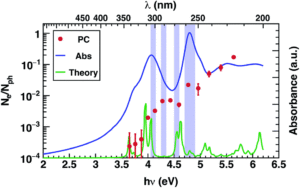
Comparison of photoconductivity, optical absorption and theoretical calculation of coranulenne. From RSC Adv.

We have been measuring photoconductivity spectra in non-crystalline corannulene thin layers and compared them to optical absorption in solution phase and thin films. The unexpected enhanced photoconductivity is correlated with GW–BSE theoretical predictions of corannulene gas-phase excitonic spectra. Theoretical analysis reveals a consistent contribution involving transitions to Super Atomic Molecular Orbitals (SAMOs), a unique set of diffuse orbitals typical of curved conjugated constructs. Results suggest SAMO population via direct photoexcitation as a potential mechanism towards exploiting these diffuse orbitals as conducting channels in suitably assembled quantum nanostructures or solids. Results are published in RSC Advances.

Posted in Uncategorized | Leave a comment

Role of transport band edge variation on delocalized charge transport in high-mobility crystalline organic semiconductors

Fast photoconductivity response of single crystal of BT8BT

Thorough investigation of fast charge transport through large single-crystal organic semiconducting layers elucidated a new type of charge transport. Together with colleagues from Belgium, Ukraine, Slovenia and Germany, we demonstrate that the degree of charge delocalization has a strong impact on polarization energy and thereby on the position of the transport band edge in organic semiconductors. This gives rise to long-range potential fluctuations, which govern the electronic transport through delocalized states in organic crystalline layers. This concept is employed to formulate an analytic model that explains a negative field dependence coupled with a positive temperature dependence of the charge mobility observed by a lateral time-of-flight technique in a high-mobility crystalline organic layer. This has important implications for the further understanding of the charge transport via delocalized states in organic semiconductors. More in PRB here.

Posted in Uncategorized | Leave a comment

Interface-controlled growth of organic semiconductors on graphene

PDIF-CN2 on graphene

We have studied submonolayer coverages of N,N-1H,1H-perfluorobutyl dicyanoperylenecarboxydiimide (PDIF-CN2) on mechanically exfoliated graphene transferred onto SiO2 substrates. Our atomic force microscopy (AFM) data show that PDIF-CN2 forms irregularly-shaped 1.4  nm-high islands. From the selected area diffraction performed with transmission electron microscope (TEM) we conclude that this height corresponds to stacks of molecules, which are inclined for 43° relative to the graphene surface. AFM also showed complete absence of PDIF-CN2 on single-layer graphene (SLG). Electric force microscopy revealed a marked difference in surface charge density between a single-layer graphene and bilayer graphene, with a higher surface charge on SLG than on the bilayer graphene. We associate this behavior with type doping of graphene due to the electrostatic dipole induced by the molecular water layer present at the graphene/SiO2 interface. The crucial role of the graphene/SiO2 interface in determining growth of PDIF-CN2 was further confirmed by TEM examination of PDIF-CN2 deposited onto unsupported SLG. The results are published in Surface Science.

Posted in Uncategorized | Leave a comment

Fast-Response Photonic Device Based on Organic-Crystal Heterojunctions Assembled into a Vertical-Yet-Open Asymmetric Architecture

Schematic view of photonic device based on vertical organic nanowires

Organic semiconductor, due to their excellent interaction with light, could be made into photosensors. The scientists of the Laboratory of Organic Physics have been working together with colleagues from University of Strasbourg and CNR Bologna on novel forms of photonic devices. In these, crystalline dioctyl-3,4,9,10-perylenedicarboximide nanowires and 6,13-bis(triisopropylsilylethynyl) pentacene microplates are integrated into a vertical-yet-open asymmetrical heterojunction for the realization of a high-performance organic photovoltaic detector, which shows fast photoresponse, ultrahigh signal-to-noise ratio, and high sensitivity to weak light. The results are published in Advanced Materials.

Posted in Uncategorized | Leave a comment