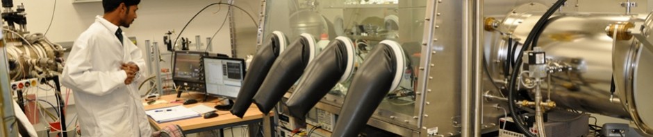
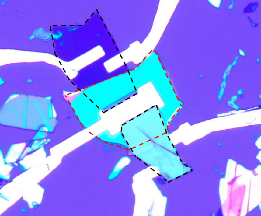
 Our researchers were involved in the research of electrical interfaces to two-dimensional semiconductors. The outcome of collaboration was a surprising finding, which was published in Nanomaterials. The two-dimensional semiconductor material under research was tungsten diselenide (WSe2), which has emerged as a promising ambipolar semiconductor material for field-effect transistors (FETs) due to its unique electronic properties, including a sizeable band gap, high carrier mobility, and remarkable on–off ratio. However, engineering the contacts to WSe2 remains an issue, and high contact barriers prevent the utilization of the full performance in electronic applications. Furthermore, it could be possible to tune the contacts to WSe2 for effective electron or hole injection and consequently pin the threshold voltage to either conduction or valence band. This would be the way to achieve complementary metal–oxide–semiconductor devices without doping of the channel material.This study investigates the behaviour of two-dimensional WSe2 field-effect transistors with multi-layer palladium diselenide (PdSe2) as a contact material. We demonstrate that PdSe2 contacts favour hole injection while preserving the ambipolar nature of the channel material. This consequently yields high-performance p-type WSe2 devices with PdSe2 van der Waals contacts. Further, we explore the tunability of the contact interface by selective laser alteration of the WSe2 under the contacts, enabling pinning of the threshold voltage to the valence band of WSe2, yielding pure p-type operation of the devices. See more in Nanomaterials.
Archives
- May 2026
- January 2026
- May 2025
- July 2024
- March 2024
- August 2023
- June 2023
- November 2021
- April 2021
- March 2021
- January 2021
- December 2020
- September 2020
- May 2020
- December 2018
- November 2017
- September 2017
- August 2017
- March 2017
- January 2017
- October 2016
- June 2016
- October 2015
- March 2015
- October 2014
- April 2014
- January 2014
- June 2013
- May 2013
- January 2013
- September 2012
- July 2012
- June 2012