
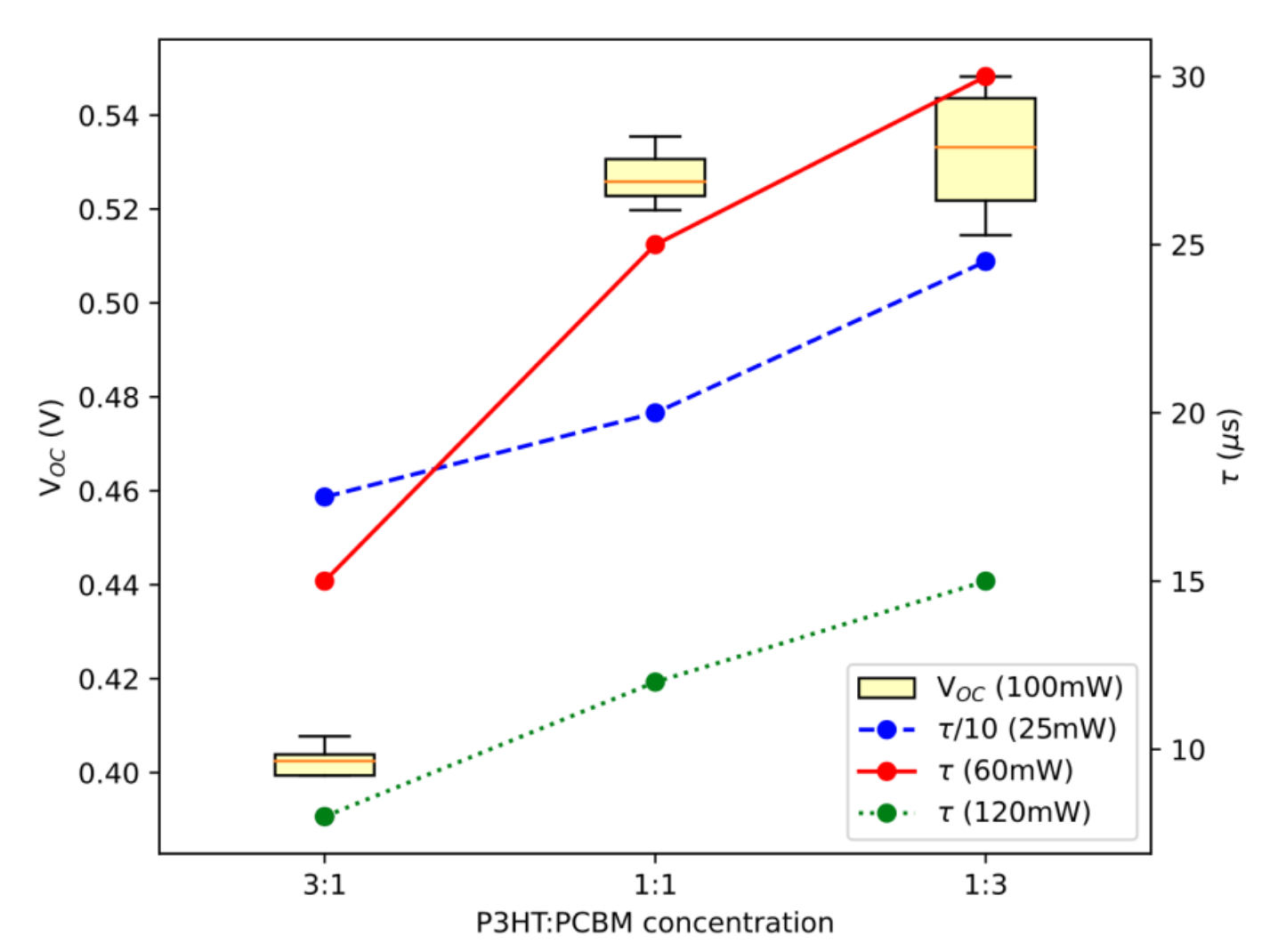
 Our researchers were measuring the performance of organic solar cells in order to validate a novel experimental method, which can be used to study the non-radiative recombination processes. In details, the influence of P3HT:PCBM ratio on thermal and transport properties of solar cells were determined by photothermal beam deflection spectrometry, which is advantageous tool for nondestructively study of bulk heterojunction layers of organic solar cells. P3HT:PCBM layers of different P3HT:PCBM ratios were deposited on top of PEDOT:PSS/ITO layers which were included in organic bulk-heterojunction solar cells. The thermal diffusivity, energy gap and charge carrier lifetime were measured at different illumination conditions and with a different P3HT:PCBM ratios. As expected, it was found that the energy band gap depends on the P3HT:PCBM ratio. Thermal diffusivity is decreasing, while charge carrier lifetime is increasing with PCBM concentration. Energy band gap was found to be independent on illumination intensity, while thermal diffusivity was increasing and carrier lifetime was decreasing with illumination intensity. The carrier lifetime exhibits qualitatively similar dependence on the PCBM concentration when compared to the open-circuit voltage of operating solar cells under AM1.5 illumination. BDS and standard I-V measurement yielded comparable results arguing that the former is suitable for characterization of organic solar cells. Results were published in https://doi.org/10.3390/ma16020617.
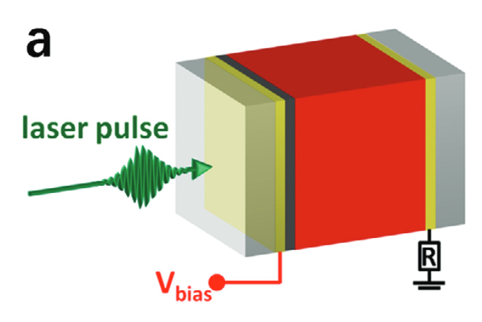 We measured record high charge mobility in a mm-sized organic semiconductors. Semiconducting mesocrystalline bulk polymer specimens that exhibit nearintrinsic properties using channel-die pressing are demonstrated. A predominant edge-on orientation is obtained for poly(3-hexylthiophene-2,5-diyl) (P3HT) throughout 2 mm-thick/wide samples. This persistent mesocrystalline arrangement at macroscopic scales allows reliable evaluation of the electronic charge transport anisotropy along all three crystallographic axes, with high mobilities found along the π-stacking. Indeed, charge-carrier mobilities of up to 2.3 cm2/Vs are measured along the π-stack, which are some of the highest mobilities reported for polymers at low charge-carrier densities (drop-cast films display mobilities of maximum ≈10−3 cm2/Vs). The structural coherence also leads to an unusually well-defined photoluminescence line-shape characteristic of an H-aggregate (measured from the surface perpendicular to the materials flow), rather than the typical HJ-aggregate feature usually found for P3HT. The approach is widely applicable: to electrical conductors and materials used in n-type devices, such as poly{[N,N′-bis(2-octyldodecyl)-naphthalene-1,4,5,8-bis(dicarboximide)2,6-diyl]-alt-5,5′-(2,2′-bithiophene)} (N2200) where the mesocrystalline structure leads to high electron transport along the polymer backbones (≈1.3 cm2/Vs). This versatility and the broad applicability of channel-die pressing signifies its promise as a straightforward, readily scalable method to fabricate bulk semiconducting polymer structures at macroscopic scales with properties typically accessible only by the tedious growth of single crystals. More in
 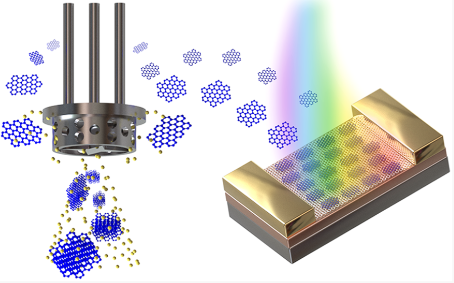 Our group has been involved in an interesting study of the photoconductivity of solution-processed nanographene ad-layers. Sensitization of graphene with inorganic semiconducting nanostructures has been demonstrated as a powerful strategy to boost its optoelectronic performance. However, the limited tunability of optical properties and toxicity of metal cations in the inorganic sensitizers prohibits their widespread applications, and the in-depth understanding of the essential interfacial charge-transfer process within such hybrid systems remains elusive. Here, we design and develop high-quality nanographene (NG) dispersions with a large-scale production using high-shear mixing exfoliation. The physisorption of these NG molecules onto graphene gives rise to the formation of graphene−NG van der Waals heterostructures (VDWHs), characterized by strong interlayer coupling through π−π interactions. As a proof of concept, photodetectors fabricated on the basis of such VDWHs show ultrahigh responsivity up to 4.5 × 10⁷ A/W and a specific detectivity reaching 4.6 × 10¹³ Jones, being competitive with the highest values obtained for graphene-based photodetectors. The outstanding device characteristics are attributed to the efficient transfer of photogenerated holes from NGs to graphene and the long-lived charge separation at graphene−NG interfaces (beyond 1 ns), as elucidated by ultrafast terahertz (THz) spectroscopy. These results demonstrate the great potential of such graphene−NG VDWHs as prototypical building blocks for high-performance, low-toxicity optoelectronics. The study is published in
 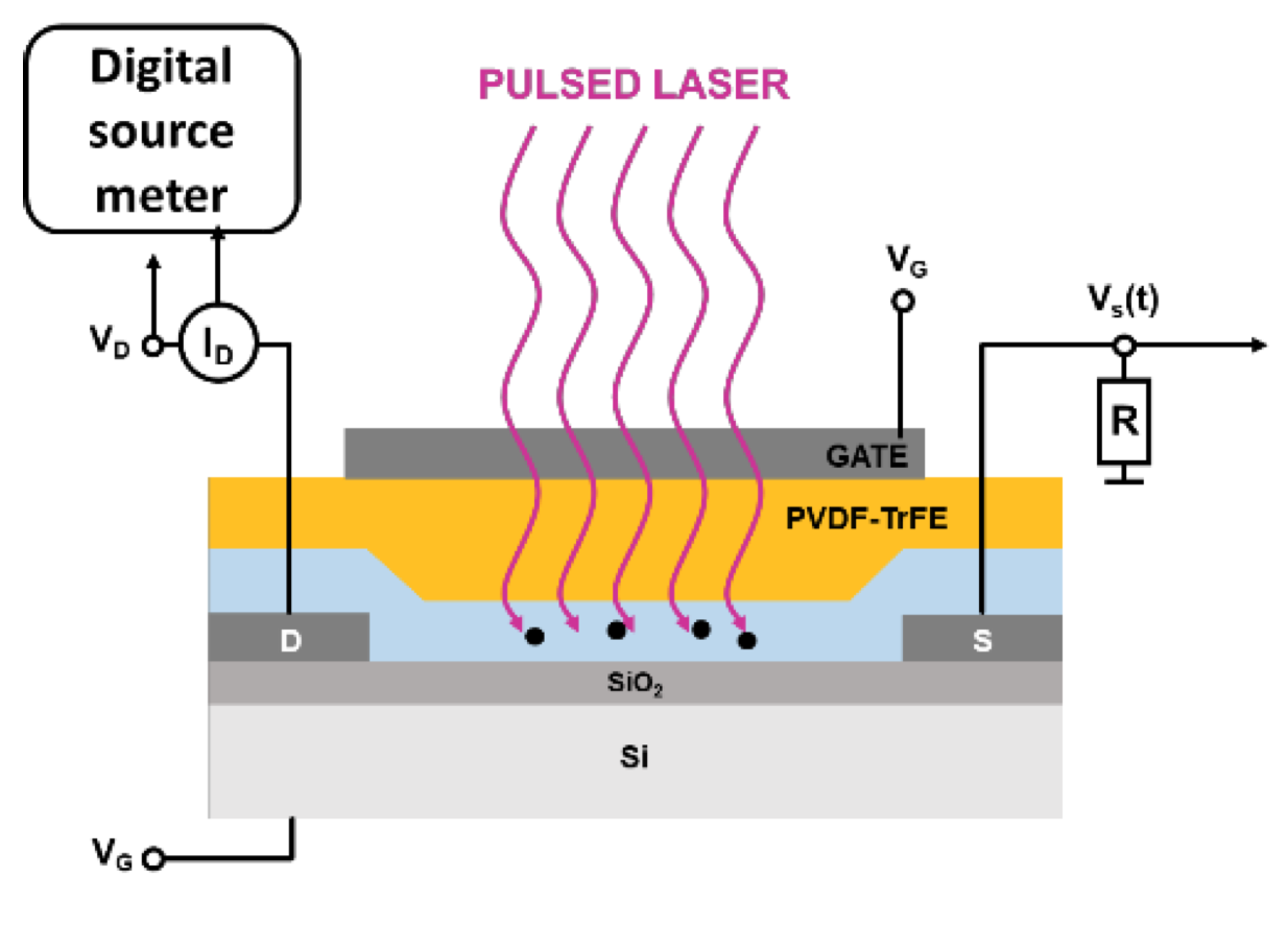 Our group was involved in research of novel type of organic transistors. Organic transistors are key elements for flexible, wearable, and biocompatible logic applications. Multiresponsivity is highly sought‐after in organic electronics to enable sophisticated operations and functions. Such a challenge can be pursued by integrating more components in a single device, each one responding to a specific external stimulus. Here, the first multiresponsive organic device based on a photochromic–ferroelectric organic field‐effect transistor, which is capable of operating as nonvolatile memory with 11 bit memory storage capacity in a single device, is reported. The memory elements can be written and erased independently by means of light or an electric field, with accurate control over the readout signal, excellent repeatability, fast response, and high retention time. Such a proof of concept paves the way toward enhanced functional complexity in optoelectronics via the interfacing of multiple components in a single device, in a fully integrated low‐cost technology compatible with flexible substrates. These findings were published in
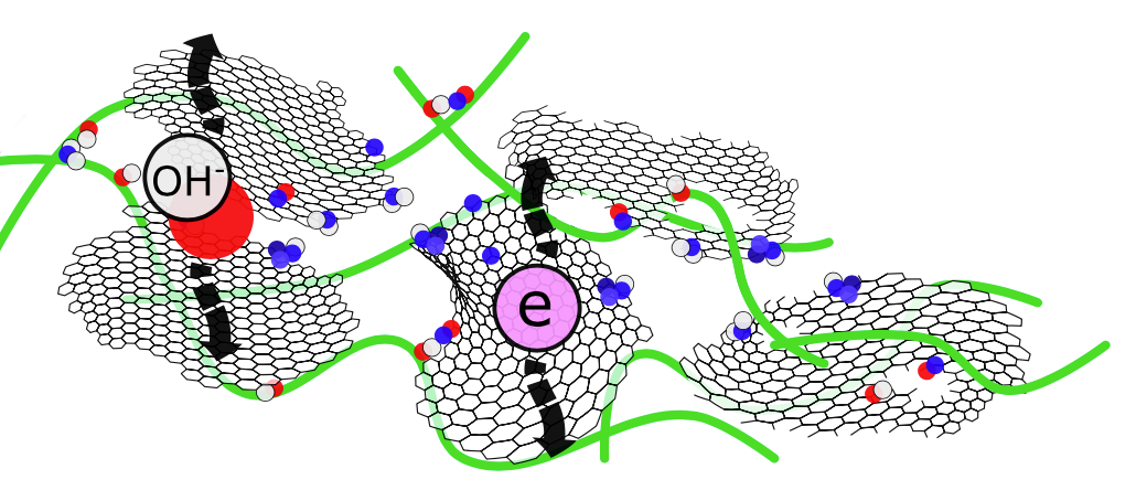
Archives
- May 2026
- January 2026
- May 2025
- July 2024
- March 2024
- August 2023
- June 2023
- November 2021
- April 2021
- March 2021
- January 2021
- December 2020
- September 2020
- May 2020
- December 2018
- November 2017
- September 2017
- August 2017
- March 2017
- January 2017
- October 2016
- June 2016
- October 2015
- March 2015
- October 2014
- April 2014
- January 2014
- June 2013
- May 2013
- January 2013
- September 2012
- July 2012
- June 2012