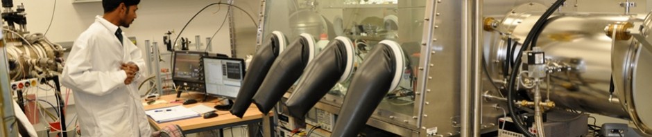
With this microscope, we can conduct nanoscale characterization of materials’ surface typology and properties.
This equipment combines high-resolution surface imaging with detailed electrical and work function measurements, offering versatile analysis for a wide range of materials.
The Kelvin Probe Force Microscopy (KPFM) mode enables non-contact potential mapping, providing insights into the electronic properties of materials. This technique is particularly useful for studying work function variations, charge distribution, and surface dipole layers.
Key features:
Monoatomic step resolution even with 100 x 100 μm scanner
High accuracy in repositioning over all scanning range with no border distortion
High Sensitivity for low force measurements
Best for soft materials
Modular structure capable to provide different scanning probe modes.
Resolution:
X-Y scan size: 0.4 nm (High voltage closed loop), 0.1 nm (High voltage open loop)
Z scan size: 0.1 nm (high voltage mode), 0.01 nm (low voltage mode)
Archives
- July 2026
- May 2026
- January 2026
- May 2025
- July 2024
- March 2024
- August 2023
- June 2023
- November 2021
- April 2021
- March 2021
- January 2021
- December 2020
- September 2020
- May 2020
- December 2018
- November 2017
- September 2017
- August 2017
- March 2017
- January 2017
- October 2016
- June 2016
- October 2015
- March 2015
- October 2014
- April 2014
- January 2014
- June 2013
- May 2013
- January 2013
- September 2012
- July 2012
- June 2012