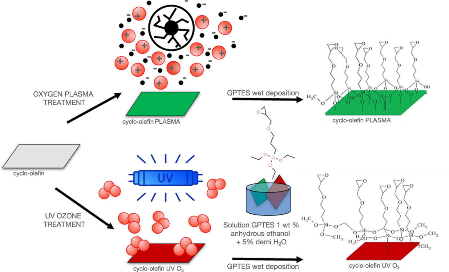
 We have been involved in an interesting study related to bio-sensing applications. In details, cyclo-olefin-copolymer (COC) transparent films are currently the best choice for micro-fluidic bio-sensors for point-of-care diagnostic applications using optical signal detection. However, while the optical and mechanical properties of this polymer are extremely good, the adhesion of the bio-probes on this surface is not optimal, due to its chemical structure, that presents only saturated carbon bonds. The deposition of organo-silane molecules on the COC surface is one of the most effective ways to overcome this problem. But, for the surface functionalization, a surface physical treatment is necessary before the chemical modification of the COC surface. In this paper a comparison of the effectiveness of two different physical treatments, oxygen plasma and UV-ozone, is reported. In particular, the exposure time of the UV-Ozone treatment has been selected to avoid the problem of auto-fluorescence of the modified COC surface, that was observed also for relatively short UV exposure (around 10 min). An investigation of the reactive radicals created on the surface after the physical treatments and the following chemical modification with the organo-silane molecule (GPTES) has been performed using X-ray photoemission spectroscopy. The surface energy and morphology of the films have been also measured by contact angle and optical profilometry. Finally, the bio-probes adhesion performances of the COC surfaces obtained with the two physical treatments and the chemical modification were tested in a fluorescence-based assay, using an organic light emission diode to excite the fluorescence. We observed that the UV-ozone treatment allows to obtain a siloxane network with some reactive epoxy radicals on the COC surface, however, their quantity and distribution are less important and homogeneous than in the oxygen plasma treated surfaces. This work is published in Surfaces and Interfaces
Volume 51, August 2024, 104663
We have been involved in an interesting study related to bio-sensing applications. In details, cyclo-olefin-copolymer (COC) transparent films are currently the best choice for micro-fluidic bio-sensors for point-of-care diagnostic applications using optical signal detection. However, while the optical and mechanical properties of this polymer are extremely good, the adhesion of the bio-probes on this surface is not optimal, due to its chemical structure, that presents only saturated carbon bonds. The deposition of organo-silane molecules on the COC surface is one of the most effective ways to overcome this problem. But, for the surface functionalization, a surface physical treatment is necessary before the chemical modification of the COC surface. In this paper a comparison of the effectiveness of two different physical treatments, oxygen plasma and UV-ozone, is reported. In particular, the exposure time of the UV-Ozone treatment has been selected to avoid the problem of auto-fluorescence of the modified COC surface, that was observed also for relatively short UV exposure (around 10 min). An investigation of the reactive radicals created on the surface after the physical treatments and the following chemical modification with the organo-silane molecule (GPTES) has been performed using X-ray photoemission spectroscopy. The surface energy and morphology of the films have been also measured by contact angle and optical profilometry. Finally, the bio-probes adhesion performances of the COC surfaces obtained with the two physical treatments and the chemical modification were tested in a fluorescence-based assay, using an organic light emission diode to excite the fluorescence. We observed that the UV-ozone treatment allows to obtain a siloxane network with some reactive epoxy radicals on the COC surface, however, their quantity and distribution are less important and homogeneous than in the oxygen plasma treated surfaces. This work is published in Surfaces and Interfaces
Volume 51, August 2024, 104663
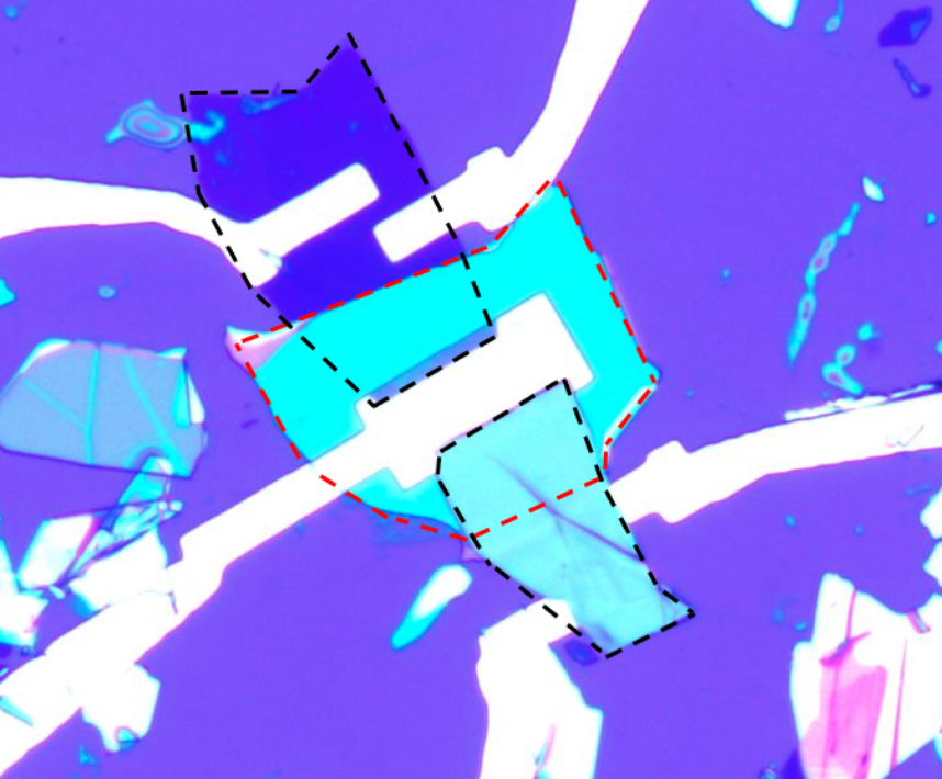 Our researchers were involved in the research of electrical interfaces to two-dimensional semiconductors. The outcome of collaboration was a surprising finding, which was published in
 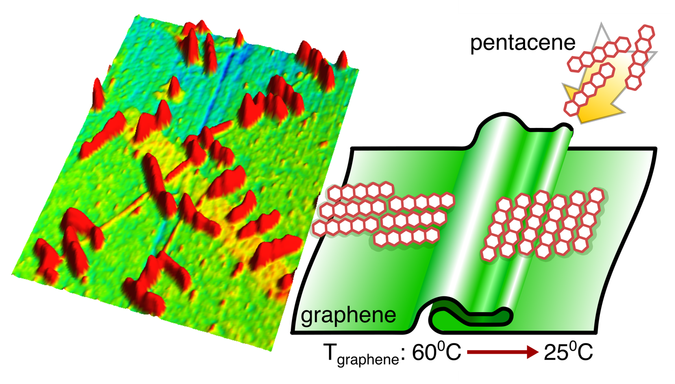 Using atomic force microscopy, we probed growth of pentacene molecules on graphene that was fabricated by chemical vapor deposition (CVD) and transferred onto 300 nm-thick SiO2 substrates. We observe that the folds on CVD graphene act as a potential barrier for the surface transport of pentacene molecules. They are oriented either parallel or perpendicular to the folds, they are also predominantly oriented along the symmetry axes of graphene. Orientation of pentacene islands on graphene evaporated at room temperature has a wide distribution. On the contrary, most of the pentacene islands evaporated at 60°C are oriented at 30° with respect to the fold direction. In addition, we interpret the 3D growth of pentacene islands on graphene in terms of reduced polar components of surface energy on graphene investigated with contact angle measurements. The results were published in
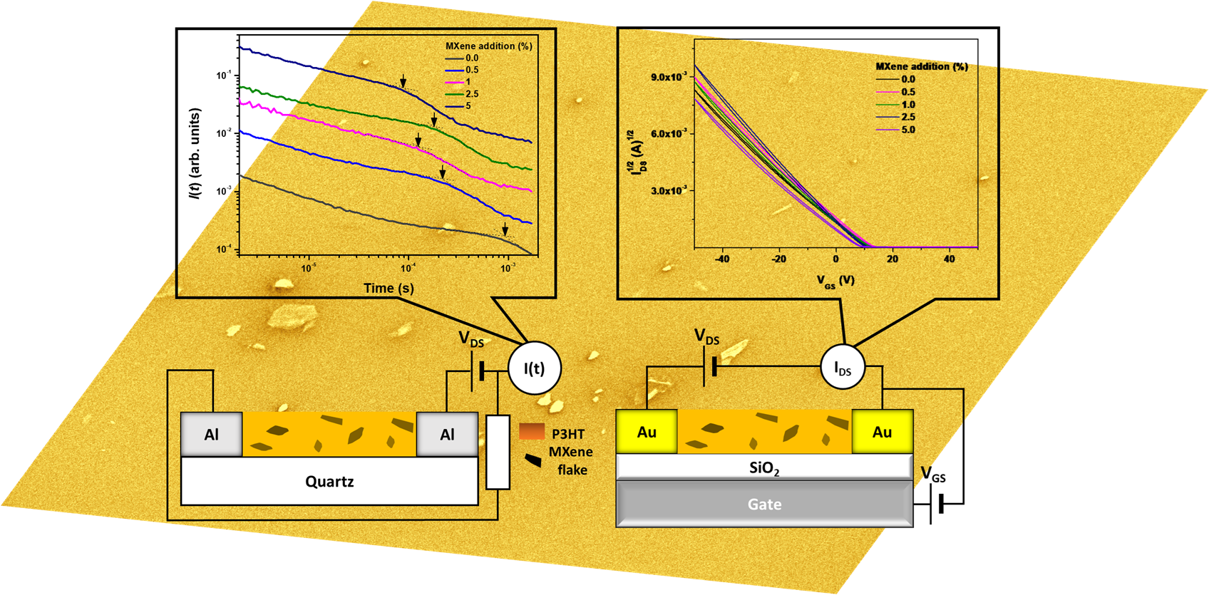
 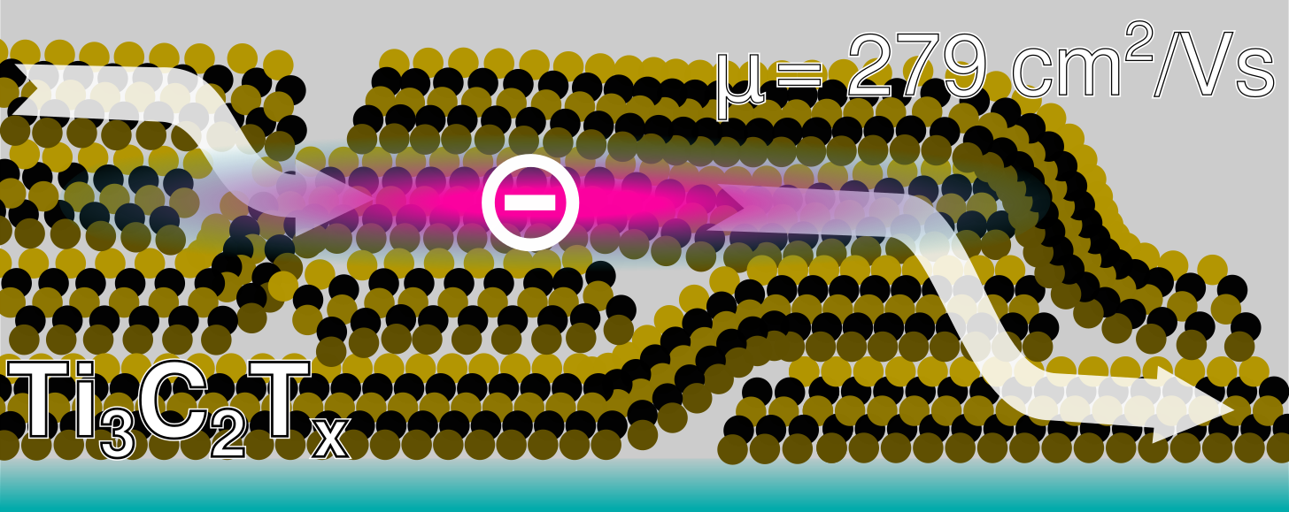 We measured record-high charge mobility in randomly oriented multilayered network of two-dimensional (2D) Ti3C2Tx (where Tx is the surface termination and corresponds to O, OH and F) was studied using time-of-flight photoconductivity (TOFP) method, which is highly sensitive to the distribution of charge carrier velocities. We prepared samples comprising Ti3C2Tx with thickness of 12 nm or 6-monolayers. MXene flakes of size up to 16 μm were randomly deposited on the surface by spin-coating from water solution. Using TOFP, we have measured electron mobility that reached values up to 279 cm2/Vs and increase with electric-field in a Poole-Frenkel manner. These values are approximately 50 times higher than previously reported field-effect mobility. Interestingly, our zero-electricfield extrapolate approaches electron mobility measured using terahertz absorption method, which represents intra-flake transport. Our data suggest that macroscopic charge transport is governed by two distinct mechanisms. The high mobility values are characteristic for the intra-flake charge transport via the manifold of delocalized states. On the other hand, the observed Poole-Frenkel dependence of charge carrier mobility on the electric field is typical for the disordered materials and suggest the existence of an important contribution of inter-flake hopping to the overall charge transport. Results were published in
  We are seeking a talented PhD student to join our team and experimentaly investigate the electro-optical properties of 2D heterostructures and organic semiconductors. The ideal candidate will have a strong background in solid state physics and intuition to perform experimental research. The successful candidate will be responsible for developing and implementing advanced techniques for characterizing the properties of these materials, as well as for designing and conducting experiments to gain deeper insights into their behavior. The candidate will learn how to prepare 2D heterostructures including organic semiconductors and study their applicability by preparing novel electronic components, organic thin film transistors, photodetectors, organic solar cells, memory components, energy-harvesting components, and bio-mimetic components e.g. biosensors. The selected candidate will be immediately employed and involved in the experimental research in
 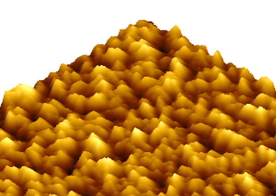 Direct alkaline ethanol fuel cells are showing promising improvements. In this brief communication, we have presented atomic force microscopy of fuel cell membranes, enhanced with graphene-oxide nanoparticles. More in
 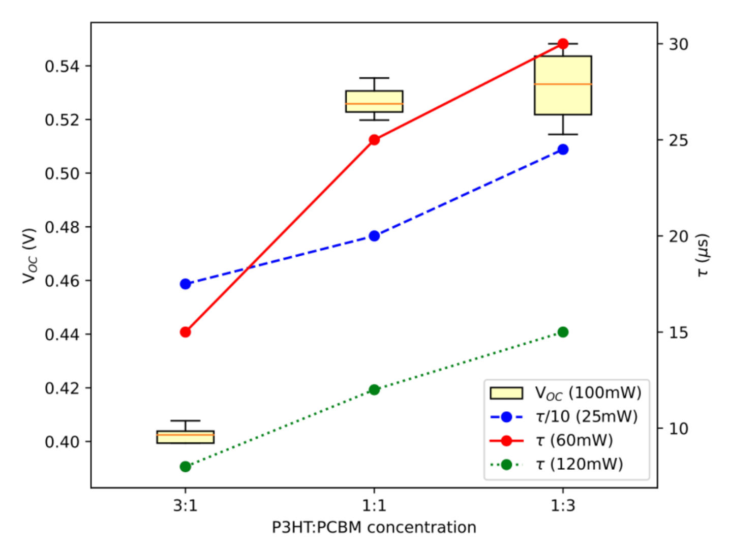 Our researchers were measuring the performance of organic solar cells in order to validate a novel experimental method, which can be used to study the non-radiative recombination processes. In details, the influence of P3HT:PCBM ratio on thermal and transport properties of solar cells were determined by photothermal beam deflection spectrometry, which is advantageous tool for nondestructively study of bulk heterojunction layers of organic solar cells. P3HT:PCBM layers of different P3HT:PCBM ratios were deposited on top of PEDOT:PSS/ITO layers which were included in organic bulk-heterojunction solar cells. The thermal diffusivity, energy gap and charge carrier lifetime were measured at different illumination conditions and with a different P3HT:PCBM ratios. As expected, it was found that the energy band gap depends on the P3HT:PCBM ratio. Thermal diffusivity is decreasing, while charge carrier lifetime is increasing with PCBM concentration. Energy band gap was found to be independent on illumination intensity, while thermal diffusivity was increasing and carrier lifetime was decreasing with illumination intensity. The carrier lifetime exhibits qualitatively similar dependence on the PCBM concentration when compared to the open-circuit voltage of operating solar cells under AM1.5 illumination. BDS and standard I-V measurement yielded comparable results arguing that the former is suitable for characterization of organic solar cells. Results were published in